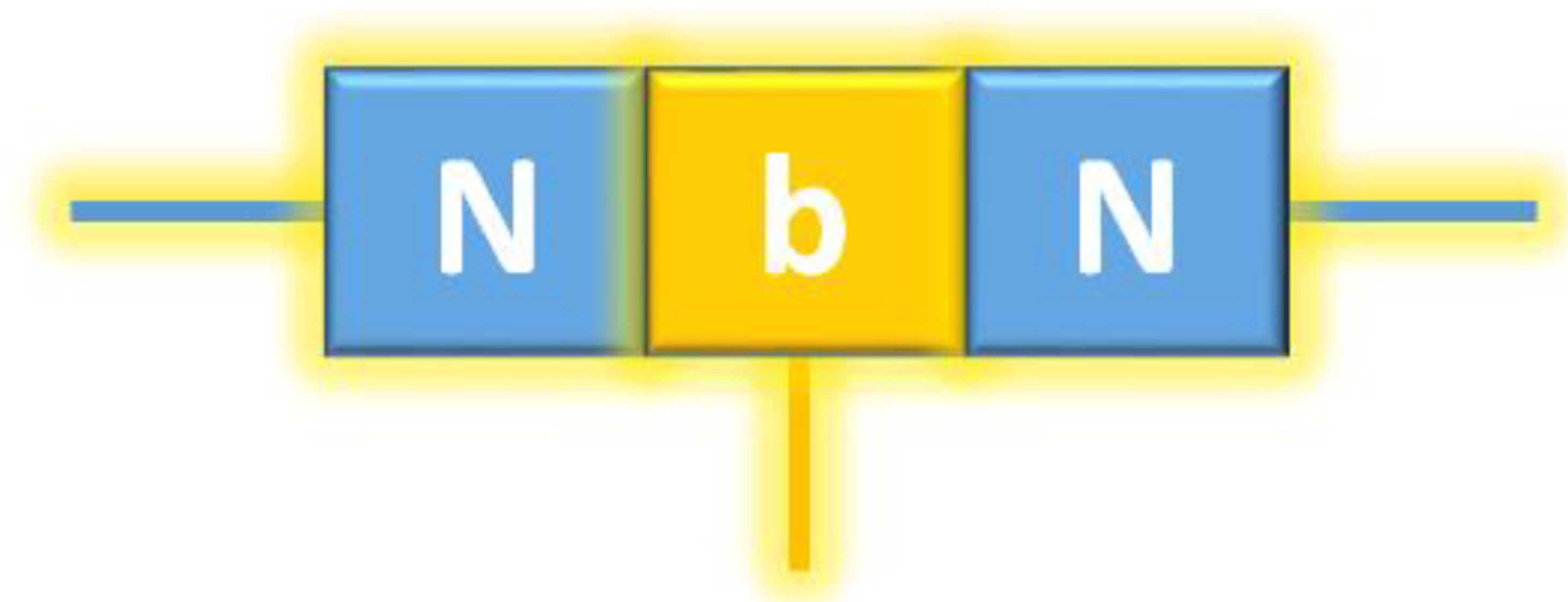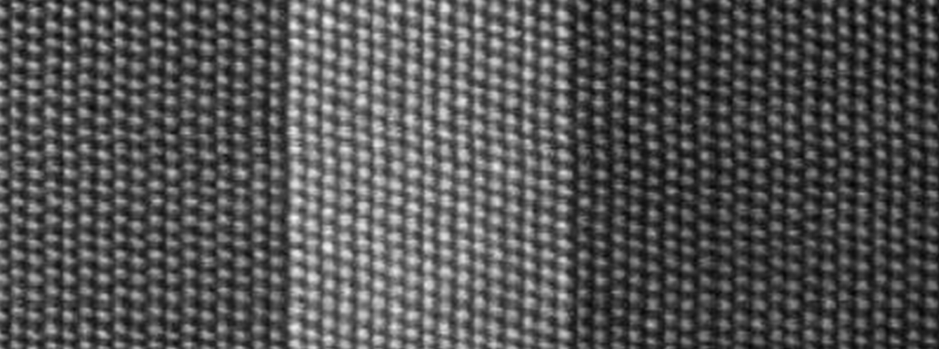

Niobium Nitride (NbN) is a metal at room temperature.
The Niobium project aims to realize a first demonstration of a Metal-Based Transistor (MBT) using III-Nitride (III-N) semiconductor materials.
The key issue is to develop an original III-N/ Metallic NbN /III-N heterostructure, using epitaxy.
Although Gallium Nitride High Electron Mobility Transistors (HEMTs) have been investigated over the last 20 years,
their lateral geometry turns out to be a disadvantage for increasing the operating frequencies.
Vertical geometry transistors may overcome several limits of the High Electron Mobility Transistors (HEMT) for two mains reasons:
Moreover there are many other areas of physics that will benefit from the results of the Niobium project, such as:
The originality of the project relies mostly on the complementary background and expertises of
III-V Lab, CRHEA and CIMAP.
| LEGAL INFORMATION | SITE MAP |