Partner 1 : III-V Lab
III-V Lab is a private R&D organisation jointly established by Nokia, Thales and the CEA under the French “Economic Interest Grouping”
(GIE) status and is located in Palaiseau, about 25 km south of Paris.
The mission of III-V Lab is to perform research and development on III-V semiconductor components, and integration with Si circuits and micro-systems,
from basic research to technology transfer for industrialisation, or to small scale and pilot line production.
III-V Lab takes advantage of the commonalities between the technologies developed for different markets addressed by Thales and Nokia,
such as telecom, space, defence and security.
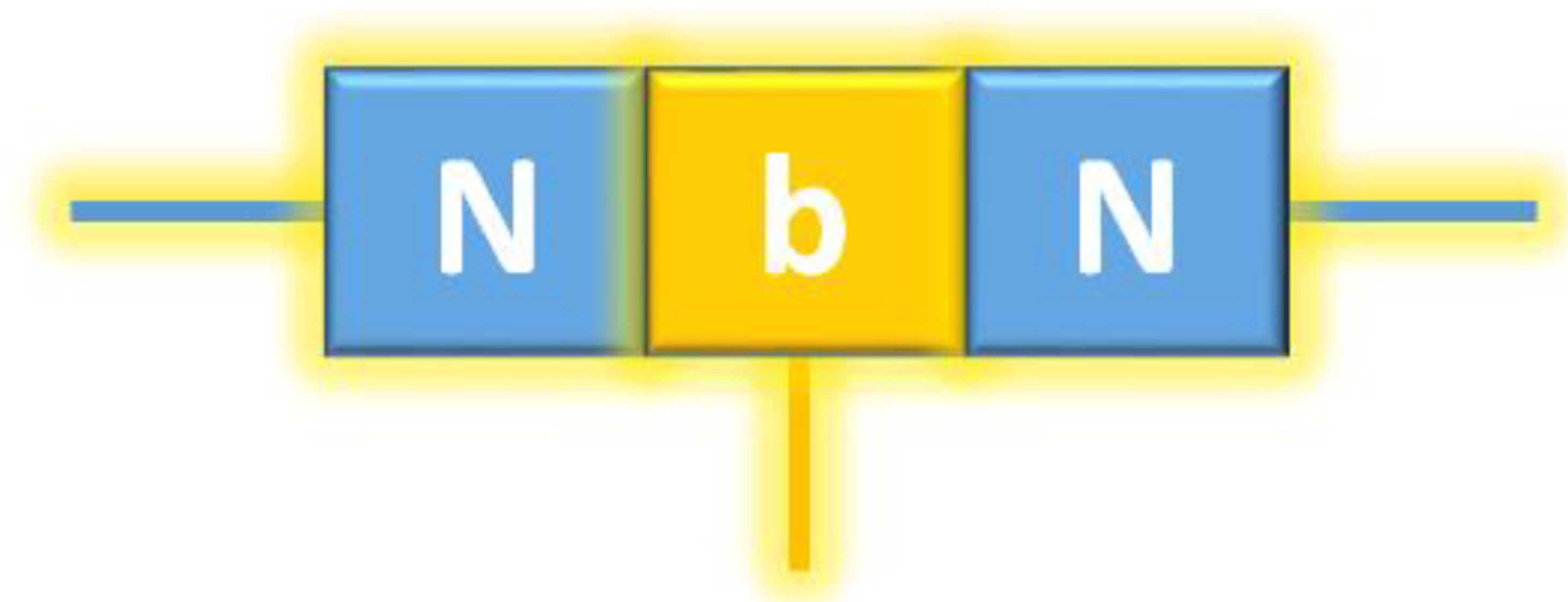
III-V Lab has a long history and a strong know-how in the field of vertical geometry semiconductor devices, and filled a patent about the realization of a high-performance metal-based transistor in the III-N
semiconductor family. The GaN activities involve MOVPE growth, GaN processing, advanced lithography, and microwave ones.
Project contact (coordinator): nicolas.michel@3-5lab.fr |
